Transistors: the building blocks of our digital world
Transistors are semiconductor devices that regulate the flow of electrical current within a circuit. Their invention in the mid-20th century marked a pivotal moment in electronics. Semiconductors, typically made of silicon or germanium, form the basis of transistors, granting them the ability to switch and amplify electrical signals. These devices have revolutionized the world of electronics, making way for the digital age by enabling the miniaturization of complex circuits and facilitating the rapid advancement of technology.
Components
| Transistor
|

Transistors categorization
Transistors are typically categorized into two main families based on their construction and operation:
Bipolar Junction Transistors (BJTs): this family of transistors includes NPN (negative-positive-negative) and PNP (positive-negative-positive) types. They consist of three semiconductor layers and are used as current amplifiers and switches in various electronic applications.
Field-Effect Transistors (FETs): FETs are another major family of transistors and are classified into two main types: MOSFETs (Metal-Oxide-Semiconductor FETs) and JFETs (Junction FETs). FETs rely on an electric field to control the flow of current, and they are widely used in microprocessors, memory chips, amplifiers, and other electronic circuits.
These two families represent the fundamental types of transistors used in modern electronics. Each family has its own subtypes and variations, offering different characteristics and capabilities to suit various applications.
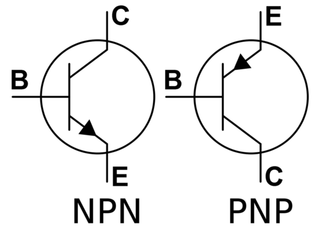
Bipolar Junction Transistor - BJT
A Bipolar Junction Transistor is a type of transistor that consists of three semiconductor layers. These layers are doped differently to create two junctions between them, hence the name bipolar. BJTs come in two polarities: NPN (negative-positive-negative) and PNP (positive-negative-positive). The NPN and PNP BJTs have the same basic structure, but the direction of the current flow and the types of charge carriers (electrons or holes) differ between them.
The three pins or terminals of a BJT are as follows:
Emitter (E): the emitter is heavily doped (either with excess electrons for NPN or excess holes for PNP) and is the source of majority charge carriers. It releases or emits the charge carriers into the base region.
Base (B): the base is lightly doped and controls the flow of charge carriers from the emitter to the collector. By applying a small current to the base, the flow of charge carriers between the emitter and collector is regulated.
Collector (C): the collector is moderately doped and collects the majority charge carriers that flow from the emitter to the base. It allows the current to pass through the transistor and is responsible for the output of the transistor.
In an NPN transistor, the current flows from the emitter to the collector when a small current is applied to the base. In a PNP transistor, the current flows from the collector to the emitter when a small current is applied to the base. This control of current flow through the base terminal is what enables the BJT to function as an amplifier or a switch in various electronic circuits.
BJTs are commonly used in applications such as audio amplifiers, signal processing circuits, voltage regulators, and digital logic circuits. They are versatile and have been a crucial component in electronics for decades, playing a vital role in powering numerous electronic devices we use in our daily lives.
Field-Effect Transistor - FET
A Field-Effect Transistor is another type of transistor that relies on an electric field to control the flow of current. FETs are known for their high input impedance, which makes them suitable for many electronic applications, especially in integrated circuits. FETs are broadly classified into two main types: MOSFETs (Metal-Oxide-Semiconductor FETs) and JFETs (Junction FETs).
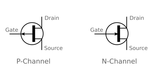
FETs have three main pins or terminals: gate, source, and drain. These pins play crucial roles in controlling the flow of current within the transistor and determining its overall functionality. The three pins or terminals of a FET are as follows:
Gate (G): the gate terminal is a key element in FETs and serves as the control terminal. In MOSFETs, the gate is insulated from the channel by a thin oxide layer, while in JFETs, the gate is directly connected to the semiconductor channel. By applying a voltage to the gate, an electric field is generated, which influences the width and conductivity of the channel. The gate terminal controls the flow of current between the source and drain terminals by modulating the conductivity of the semiconductor channel.
Source (S): the source terminal is the point of entry or exit for the majority charge carriers (either electrons or holes) in the semiconductor channel. It is the source of these charge carriers for the FET. The source terminal establishes the starting point for the flow of current through the transistor.
Drain (D): the drain terminal is where the majority charge carriers exit or enter the semiconductor channel. It acts as the endpoint for the flow of current through the transistor. When a voltage is applied to the gate, the flow of charge carriers between the source and drain terminals is regulated, allowing current to pass through the transistor.
It's important to note that FETs come in different configurations, such as N-channel and P-channel:
In N-channel, a positive voltage applied to the gate terminal creates an electric field that attracts electrons, leading to the formation of a conductive channel between the source and drain terminals.
In P-channel, a negative voltage applied to the gate terminal creates an electric field that attracts holes, forming a conductive channel between the source and drain terminals.
BJT vs FET
Bipolar Junction Transistors (BJTs) and Field-Effect Transistors (FETs) are both essential components in electronics, but their characteristics make them suitable for different applications.
BJT transistors excel in low-power and high-frequency applications, making them ideal for use in audio amplifiers, signal processing circuits, and radio frequency (RF) circuits. They also provide high current gain, making them suitable for power amplification tasks.
On the other hand, FET transistors, particularly MOSFETs, are well-suited for high-speed and low-power applications, such as in microprocessors, memory chips, and digital integrated circuits. They offer high input impedance, which reduces the load on input signals, making them favorable for high-impedance circuits. JFETs, on the other hand, are useful in high-frequency applications and low-noise amplifiers.
In summary, BJT transistors are often preferred in high-power and high-frequency applications, while FET transistors, especially MOSFETs, are more commonly used in low-power and high-speed applications where high input impedance is essential. The choice between the two types depends on the specific requirements of the circuit and the characteristics needed for the desired functionality.
Conclusion
In the ever-advancing world of technology, transistors remain a crucial component, silently shaping our daily lives. From the simplest circuits to the most sophisticated electronic devices, their versatile nature empowers innovation and drives progress. Transistors have not only made electronics faster, smaller, and more efficient but have also paved the way for groundbreaking advancements across various industries.


0 Comments