Using transistors in electronic circuits
Transistors are fundamental semiconductor devices that revolutionized the world of electronics. Among various types of transistors, Bipolar Junction Transistors (BJTs) hold significant importance due to their widespread use in amplification, switching, and signal processing applications. This article will explore the two main types of BJT transistors: NPN and PNP. We will explore their basic structures, operating principles, and essential circuit elements required for their proper functioning.
Components
| Transistor
|

Prerequisites
We highly recommend reading the article that provides an introduction to transistors: Transistors: the building blocks of our digital world.
Your BJT transistor comes with a plastic head and three small metal pins extending from one end. It's very important to identify your transistor pins before using it. We recommend that you refer to the transistor datasheet to verify the function of each pin.
BJTs operating modes
Bipolar Junction Transistors (BJTs) operate in three distinct modes: active mode, cutoff mode, and saturation mode. Each mode corresponds to specific biasing conditions that determine the behavior of the transistor. Let's explore each mode in detail:
Active Mode:
The active mode is the typical operating mode of a BJT transistor when used for amplification purposes. In this mode, the transistor is biased with a sufficient base current (Ib) to allow the flow of collector current (Ic). For an NPN transistor, this means that the base-emitter junction is forward-biased, while the base-collector junction is reverse-biased.
The forward bias on the base-emitter junction causes majority carriers (electrons for NPN transistors) to diffuse from the emitter to the base region. A small fraction of these carriers then crosses the reverse-biased base-collector junction and flows to the collector, resulting in amplified current at the collector terminal.
Cutoff Mode:
The cutoff mode occurs when there is no base current (Ib = 0) or when the base-emitter junction is reverse-biased. In this mode, the transistor is in an OFF state, and there is negligible collector current flow (Ic ≈ 0). Essentially, the transistor acts as an open switch, preventing the flow of current between the collector and the emitter.
Saturation Mode:
The saturation mode occurs when the base current (Ib) is large enough to allow the maximum possible collector current (Ic) to flow through the transistor. In this mode, both the base-emitter and base-collector junctions are forward-biased.
When the transistor is saturated, it acts as a closed switch with a low resistance between the collector and the emitter. As a result, the collector current is at its maximum value, and the transistor can no longer provide amplification.
The capability of BJTs to transition between these three modes depending on biasing conditions makes them adaptable components in a wide range of electronic circuits, enabling signal amplification, switching, and other essential functionalities in electronic devices.
NPN Transistors
NPN transistors are one of the most commonly used electronic components. They consist of three semiconductor regions: a thin P-type layer sandwiched between two N-type layers. The N-type regions serve as the emitter and collector, while the P-type region acts as the base. In an NPN transistor, when a positive voltage is applied to the base with respect to the emitter, the current flows from the collector to the emitter.
NPN Transistor circuits and parameters
To activate the transistor, a voltage of approximately 0.7V is required across the base and the emitter (VBE). Imagine you had access to a 0.7V battery; you could connect it between the base and emitter, resulting in the transistor switching on. However, since obtaining a 0.7V battery is not always feasible, we need to find an alternative solution.
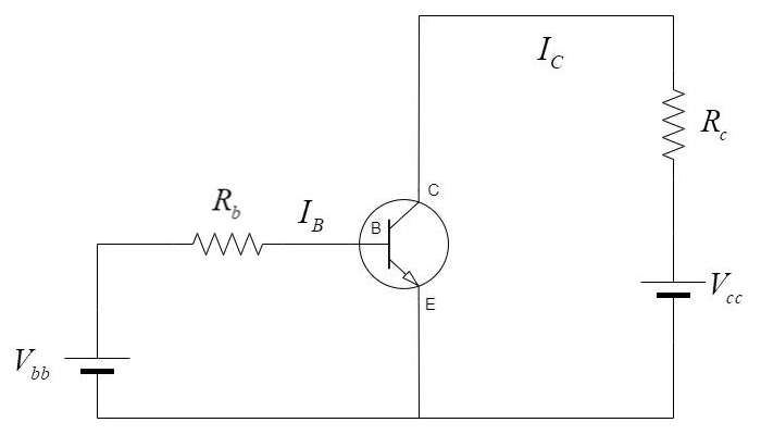
To calculate the necessary resistors for biasing an NPN transistor, you can use Ohm's law and the transistor's datasheet to find the appropriate base current and voltage. It's essential to choose resistor values that keep the transistor within its safe operating region to avoid damage. The Ohm's law formula:
V = I * R
The base-to-emitter segment of a transistor functions similarly to a diode. A diode exhibits a forward voltage, drawn from the available voltage. If a resistor is incorporated in series, the remaining voltage drop happens across the resistor. Incorporating a resistor will naturally yield around 0.7V, providing the necessary activation voltage.
Rb = (Vbb - VBE ) / Ib = (Vbb - 0.7) / Ib
When determining the values of the components, there's an additional aspect you should take into consideration about transistor operation. When a current flows from the base to the emitter, the transistor activates, allowing a larger current to move from the collector to the emitter.
Ie = Ic + Ib
A relationship exists between these two currents, known as the transistor's gain. With a transistor gain of 50, the current flowing from the collector to the emitter can be 50 times greater than the current moving from the base to the emitter.
hFe = 𝛽 (gain) = Ic / Ib
When picking a transistor, one of the primary considerations should be transistor's ability to handle current. This characteristic is referred to as the collector current (IC).
PNP Transistors
PNP transistors are similar to NPN transistors but with reversed polarities. They consist of three regions: two P-type layers separated by an N-type layer. The emitter and collector are the P-type regions, and the N-type region acts as the base. When a negative voltage is applied to the base with respect to the emitter, the current flows from the emitter to the collector. PNP transistors are also widely used in various applications, such as current mirrors and complementary circuits.
PNP Transistor circuit and parameters
Similar to NPN circuits, proper biasing using resistors is essential to ensure the transistor operates in the active region. To calculate the necessary resistors for biasing a PNP transistor, you'll follow the same principles as with NPN transistors but with reversed voltage polarities. Always refer to the transistor datasheet for accurate parameters.
Flyback diode circuit
A flyback diode, also known as a freewheeling diode or snubber diode, is a diode connected in parallel with an inductive load. Its purpose is to provide a path for the inductive current to circulate when the power supply to the load is switched off, preventing voltage spikes and protecting the circuit components.
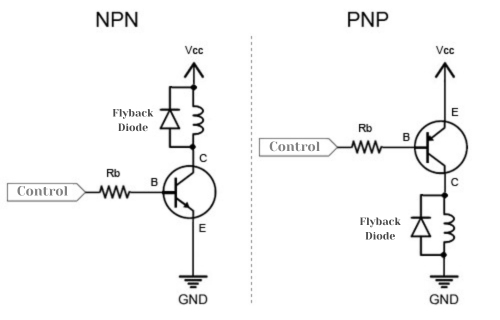
This configuration helps protect the microcontroller and other components from voltage spikes generated by the motor when it is switched off. Always refer to the datasheets of the components you are using for accurate specifications and consider the specific requirements of your motor and transistor in your circuit.
Conclusion
Bipolar Junction Transistors (BJTs) have been integral to the advancement of modern electronics. NPN and PNP transistors are the two primary types, each with its unique characteristics and applications. Understanding their basic structures, operating principles, and the proper implementation of circuits with resistors and voltages is vital. Whether it's amplification, switching, or signal processing, BJT transistors remain indispensable elements in numerous electronic systems.


0 Comments